The AI Hardware Race: Beyond Silicon—Packaging, Co-Design, and Geopolitics Defining Tomorrow’s Intelligence
The explosion of Generative AI, driven by massive Large Language Models (LLMs) and complex diffusion models, has thrown the spotlight directly onto the engine room of artificial intelligence: the chips. We often marvel at the intelligence of ChatGPT or Midjourney, but rarely do we consider the incredible physical and architectural challenges required to make that intelligence possible. If the software is the brain, the silicon is the nervous system. Based on recent analyses detailing the intricacies of AI chip fabrication, it is clear that the next breakthroughs will not come solely from shrinking transistors, but from radical shifts in packaging, software integration, and global supply chain strategy.
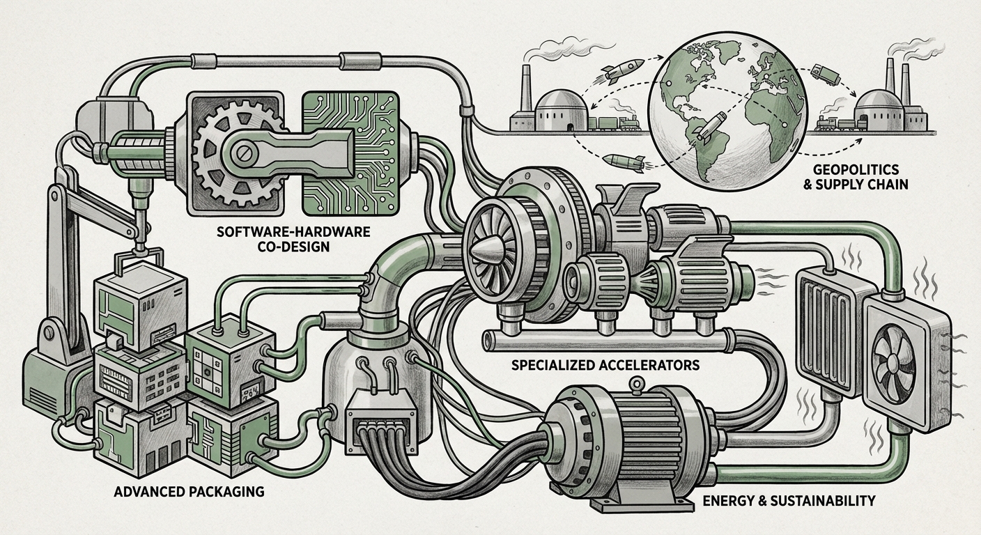
1. The End of Easy Scaling: Advanced Packaging as the New Frontier
For decades, the semiconductor industry relied on Moore’s Law—the promise that we could cram twice the number of transistors onto a chip every two years by making them smaller. While this is still attempted, we are hitting fundamental physical limits. The sheer complexity and cost of building 3-nanometer or 2-nanometer nodes means that raw scaling alone can no longer deliver the exponential performance gains needed for trillion-parameter models.
The industry pivot is toward **Advanced Packaging** and the concept of **chiplets**. Imagine a high-performance chip not as a single, massive piece of silicon, but as a set of specialized LEGO bricks built separately and then stacked or laid side-by-side using incredibly precise methods.
What This Means Technically (For Engineers):
This involves techniques like 2.5D and 3D stacking, where different functional units—like memory, high-speed logic, and I/O controllers—are bonded vertically or horizontally with micron-level precision (e.g., using TSMC’s CoWoS or Intel’s Foveros technologies). This approach allows designers to mix and match the best manufacturing process for each piece, rather than being constrained by one process for the whole chip. Performance improvements are gained not by making transistors smaller, but by drastically reducing the travel distance data has to take between components, thus increasing bandwidth and efficiency.
Implication for Business (For Executives):
This complexity raises the barrier to entry. Only a handful of foundries possess the expertise to execute advanced packaging at scale. This concentrates power and necessitates deep partnerships between AI developers (like Google or Amazon) and the specialized foundries that handle this assembly. Flexibility in design increases, but dependence on a very small number of expert manufacturing partners deepens.
2. The Symbiosis: Software-Hardware Co-Design for LLMs
A chip optimized for general computing tasks is often inefficient for the highly specific mathematics required by neural networks. Modern AI models, especially LLMs, are hungry for massive parallel processing capabilities and extremely fast access to vast amounts of memory.
Bridging the Gap Between Code and Silicon (For Developers):
Designing an AI chip is only half the battle; making software *love* that chip is the other. This convergence, known as **Software-Hardware Co-Design**, recognizes that the architecture must be tailored to the model’s structure, and vice versa. For example, if a model frequently uses sparse computations (where most values are zero), the hardware should be designed to skip those zeroes efficiently rather than wasting cycles calculating them. Articles analyzing this area often reveal how techniques like *kernel fusion*—combining several small calculation steps into one optimized chip operation—can yield huge speedups that raw transistor count cannot match.
The future means that ML frameworks (like PyTorch or TensorFlow) will need deeper integration with hardware compilers to automatically generate code perfectly suited for the target accelerator, whether it’s a giant GPU or a tiny edge device chip.
3. The Global Scramble: Geopolitics and the Concentration of Power
The sheer complexity of creating leading-edge AI chips—requiring billions of dollars for a single fabrication plant and access to highly specialized tools like Extreme Ultraviolet (EUV) lithography machines—has led to extreme geographical concentration. The majority of advanced chip manufacturing resides in East Asia, particularly Taiwan.
The Strategic Risk (For Policy Analysts):
This concentration is now viewed globally as a critical strategic vulnerability. The query around geopolitical implications highlights the urgent push, exemplified by the US CHIPS Act and similar European initiatives, to "reshore" or "friend-shore" the high-end manufacturing capabilities. If the hardware that powers global AI innovation is bottlenecked by regional instability or trade restrictions, the pace of AI progress—and economic output—stalls.
For businesses relying on cutting-edge AI, this translates into supply chain risk. Securing long-term access to foundry capacity for high-end AI accelerators is becoming as critical as securing cloud compute contracts. The hardware race is inextricably linked to national security and economic leverage.
4. Beyond the GPU: The Rise of Specialized Accelerators
While NVIDIA GPUs remain the industry workhorses, their general-purpose nature means they carry overhead that specialized chips can shed. The market is ripe for disruption from dedicated **AI Accelerators** (ASICs) designed from the ground up for specific tasks.
Targeting Niche Performance (For Investors):
The search for alternatives to GPU dominance is fierce. Startups and large tech companies (like Google with its TPUs) are building chips optimized for inference (running the model after training) or for specific model types, such as spiking neural networks or analog computing approaches. These chips promise significantly better performance per watt for defined tasks compared to general-purpose hardware.
The future will likely involve a diverse ecosystem:
- Hyperscalers (e.g., Meta, Amazon): Developing proprietary ASICs for their massive internal workloads.
- Startups: Targeting specific market segments, perhaps focusing purely on low-power edge AI deployment (smart cameras, autonomous vehicles).
- GPU Incumbents: Responding by creating highly specialized versions of their hardware tailored for specific AI libraries.
5. The Unavoidable Cost: Energy Consumption and Sustainability
All this computational muscle comes at a steep environmental cost. The energy demands of training a state-of-the-art LLM can be astronomical, and the daily operational power draw of running inference centers globally is rapidly becoming a major utility concern. The future of AI chips must be intrinsically linked to power efficiency.
Designing for a Cooler Future (For Data Center Managers):
When looking at chip operation trends, efficiency metrics like *tera operations per second per watt (TOPS/W)* are becoming more important than raw speed alone. Advances in chip design—such as better memory structures, lower voltage operations, and smart clock gating—are crucial for sustainability. Furthermore, the extreme density enabled by advanced packaging demands radical innovation in cooling infrastructure, moving towards liquid cooling solutions in data centers to manage the intense heat generated by these powerful, compact components.
Ignoring the energy cost is no longer an option. Regulatory pressure and the sheer operational expense mean that the next generation of hardware *must* deliver performance gains without proportional increases in power draw.
Actionable Insights for Navigating the Hardware Horizon
The path forward for AI development is not paved with smaller transistors alone. It requires a multi-faceted strategy built on understanding these five core pillars of hardware evolution.
For Technology Leaders:
- Diversify Hardware Strategy: Do not rely solely on one vendor or architecture. Begin benchmarking high-priority workloads across GPUs, specialized ASICs, and cloud-native accelerators to build resilience against future pricing or supply shocks.
- Invest in Compiler Talent: The performance gap between good and great in AI deployments is increasingly software-defined. Hire or train teams proficient in low-level kernel programming and hardware description languages to truly exploit custom silicon.
- Map Supply Chain Dependencies: Understand where your critical components—especially advanced packaging services—are manufactured. Develop contingency plans for potential geopolitical friction points.
For Policy and Societal Stakeholders:
- Prioritize Manufacturing Resilience: Government incentives must focus not just on R&D, but on building robust, geographically diverse, and redundant advanced packaging capacity.
- Incentivize Efficiency: Regulatory frameworks should increasingly favor AI systems that achieve high utility with low energy footprints, pushing innovation toward the TOPS/W metric over absolute peak speed.
The silicon journey from "sand to intelligence" is becoming more complex, requiring expertise spanning physics, computer science, and international relations. The race isn't just about who can build the fastest chip today, but who can master the entire ecosystem—from the chemical layers in advanced packaging to the compiler instructions driving the software—to define the accessible, efficient, and sustainable intelligence of tomorrow.