The AI Chip Monopoly: Why TSMC’s Leading Edge is Shutting Out Smartphones
The semiconductor industry has always been defined by cycles of innovation, but the current surge driven by Generative AI represents not just a cycle, but a fundamental structural pivot. Recent reports indicate that demand for advanced AI accelerators—the powerful brains powering large language models and complex digital workloads—is so overwhelming that it is effectively monopolizing the most cutting-edge production lines at Taiwan Semiconductor Manufacturing Company (TSMC).
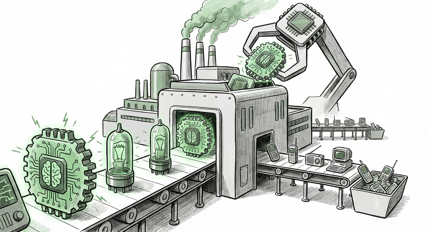
Specifically, projections suggest that by 2027, a staggering 86% of TSMC’s capacity on its most advanced nodes (like N3, the 3-nanometer process) could be dedicated solely to AI chips. This leaves traditional, high-volume consumer products, most notably smartphones, scrambling for overflow capacity. This isn't just a minor queue delay; it signifies a historical shift in technological priority. For years, the smartphone industry dictated the pace of silicon advancement. Now, the computational hunger of AI is the undisputed kingmaker.
The Bottleneck: Why AI Chips Demand the Best Real Estate
To understand this phenomenon, one must appreciate what advanced manufacturing nodes provide. Think of TSMC’s fabrication plants (fabs) as prime real estate. The newest nodes, N3 and the upcoming N2, allow engineers to cram more transistors (tiny electronic switches) into a smaller area. More transistors mean more processing power, better energy efficiency, and the ability to handle the massive parallel computations required by AI.
AI accelerators, whether they are from Nvidia, AMD, or custom designs from tech giants, are performance-at-any-cost components. They are the difference between training a cutting-edge model in three weeks versus three months. Consequently, these customers are willing to pay premiums and commit massive volumes to secure priority access to TSMC’s leading edge.
This concentration of demand validates the core concern: **AI demand is sidelining consumer electronics.** For context, smartphones have long been the primary driver for TSMC’s most advanced nodes. Now, they are being relegated to buffering overflow demand. This implies that the next generation of mobile devices might rely on slightly older, though still powerful, process technologies, potentially slowing the incremental gains in power efficiency we’ve come to expect year-over-year in flagship phones.
Corroboration: Reading the Supply Chain Tea Leaves
This reality is borne out by tracking industry data. Analysts focusing on capacity allocation confirm that the sheer volume and revenue size of AI orders have fundamentally re-written the foundry booking schedule. When major players like Nvidia book out years of capacity on N3, it inherently restricts what remains for others. This intense prioritization is what forces the wider ecosystem to adapt.
We must look beyond just the GPU manufacturers. The demand is broad:
- Nvidia & AMD: Remain the central players, ordering high-end general-purpose GPUs for data centers.
- Cloud Hyperscalers: Companies like Amazon (AWS), Google, and Microsoft are designing their own chips (ASICs) specifically optimized for their AI workloads. These custom chips still require the bleeding edge of manufacturing technology.
The Competitive Response: Foundries Race to Catch Up
When one supplier controls the market as tightly as TSMC currently does in leading-edge logic, the entire ecosystem feels the strain. This situation presents a massive opportunity—and a significant challenge—for competitors like Samsung Foundry and Intel Foundry Services (IFS).
The Search for Alternatives
If a major smartphone OEM cannot secure enough N3 capacity for their next flagship chipset, they are forced to look elsewhere. This drives two primary outcomes:
- Downgrading Node Choice: Opting for a proven, less constrained process node (like N4 or N5), accepting slight performance trade-offs for guaranteed volume.
- Seeking New Foundry Partners: Actively engaging Samsung or Intel. Samsung, for instance, is aggressively pushing its Gate-All-Around (GAA) transistor architecture to compete directly with TSMC’s FinFET successors. The success of these rivals in securing major AI contracts will determine how quickly the supply constraint eases for other industries.
For the business audience, this means supply chain risk is escalating. Relying on a single, hyper-constrained foundry exposes hardware makers to immense scheduling and pricing risk. Diversification is no longer a long-term goal; it is an immediate necessity driven by AI’s voracious appetite.
The Shift to Custom Silicon: Democratization of Chip Design
Perhaps the most profound long-term implication is the acceleration of custom silicon development. The original goal of the AI race was to run Nvidia’s GPUs efficiently. Today, the goal is optimization. Why rent an expensive, general-purpose GPU when you can design a chip perfectly tailored to *your* specific type of AI task (like image generation or text summary)?
The Rise of the AI ASIC
Hyperscalers are investing billions in developing Application-Specific Integrated Circuits (ASICs)—chips designed for one specific job. Google’s TPUs (Tensor Processing Units) are a prime example. These custom chips are designed to be perfectly efficient at running Google’s proprietary AI frameworks.
Why does this matter for manufacturing? These custom ASICs, unlike mid-range CPUs or modems, are often designed by the world’s largest tech companies specifically to utilize the absolute highest transistor density and efficiency available. They fall directly into the queue alongside Nvidia’s best products, further crowding the N3 and N2 waiting lists. This diversity of high-end demand—from merchant silicon vendors *and* captive designers—solidifies the notion that leading-edge nodes are now permanently dedicated to AI inference and training infrastructure.
Economic Justification: Following the Revenue
No manufacturer, even one as dominant as TSMC, makes capacity decisions in a vacuum. The reason for prioritizing AI accelerators boils down to simple economics: AI chips generate significantly higher revenue per wafer than almost any other component.
Market forecasts consistently show that the AI semiconductor segment is projected to grow at a blistering pace, often eclipsing the Compound Annual Growth Rate (CAGR) of traditional segments like mobile processors or PC chipsets. While a smartphone might cost $1,000, the high-end AI accelerator used to train the models fueling those phones can cost $30,000 to $40,000, with profit margins benefiting the foundry immensely.
For financial analysts and C-suite executives, this paints a clear picture: capital expenditure and capacity expansion are overwhelmingly aimed at servicing the AI infrastructure build-out. Consumer electronics, while still massive in volume, now represent a lower-margin business for the most advanced process technologies.
Actionable Insights: Navigating the New Semiconductor Landscape
This capacity constraint is not a temporary hiccup; it is the foundation of the next decade of semiconductor strategy. Here is what businesses and developers must consider:
For Hardware OEMs (Smartphones, Laptops, IoT):
- Embrace Node Migration Strategy: Accept that leading-edge features might arrive on slightly older nodes for a year or two. Future differentiation must come from software integration and specialized accelerators (like NPUs built on slightly more mature nodes) rather than raw CPU/GPU core count improvements derived from the absolute newest process.
- Secure Long-Term Capacity Locks: Engage in multi-year capacity reservation agreements now, even if it means paying higher upfront costs. The lead time for new leading-edge capacity coming online (like TSMC's N2) is measured in years, not quarters.
For AI Developers and Cloud Architects:
- Optimize for Existing Hardware: Focus development efforts on ensuring models run efficiently on current-generation hardware (like the prevalent H100/B100 generation) rather than assuming immediate access to next-next-gen chips. Efficiency is the new performance metric.
- Explore Edge AI and Specialized Compute: Look towards smaller, more specialized ASICs for deployment outside of major data centers. This offloads pressure from the primary manufacturing bottleneck while potentially improving latency and security for end-user applications.
For Foundries and Equipment Suppliers:
- Accelerate GAA/Advanced Packaging: Investment must surge into advanced manufacturing techniques like Gate-All-Around (GAA) transistors and sophisticated 3D packaging (like chiplets). These innovations are the only short-term paths to increasing performance density outside of simply migrating to the next nanometer label.
- Prioritize Foundational AI Customers: Strategic partnerships with hyperscalers and top-tier GPU providers must be solidified, as they represent the core revenue streams underpinning the massive capital investment required for advanced fab construction.
Conclusion: A New Era of Compute Hierarchy
The latest capacity data from TSMC is a flashing beacon signaling the end of one era and the dawn of another. The semiconductor hierarchy has inverted. The massive, general-purpose consumer market that once drove innovation is now secondary to the intense, focused computational demands of artificial intelligence infrastructure. This realignment forces every player—from the cloud provider designing custom silicon to the mobile phone manufacturer balancing its component budget—to fundamentally re-evaluate their technology roadmap.
The future of computing won't be defined by the fastest phone, but by the most efficient, tightly controlled manufacturing pipelines dedicated to feeding the insatiable, exponential growth of AI models. The race for lithography dominance is now fundamentally a race for AI supremacy.